Surface Mount Technology (SMT) Assembly
Capabilities Overview+ View more
Capabilities Overview
+ View more
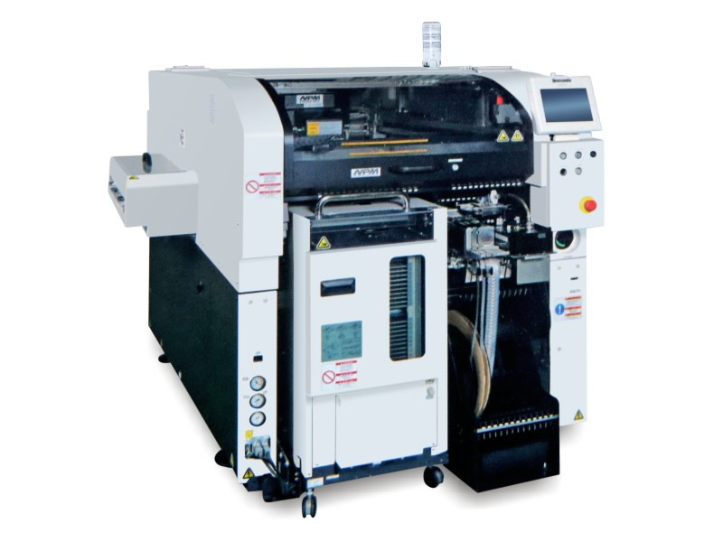
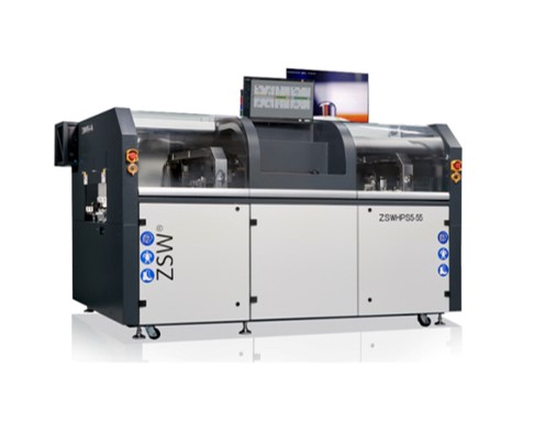
Single- and Double-Sided SMT Assembly
Placement of components on one or both sides of the PCB using automated pick-and-place machines and reflow soldering.
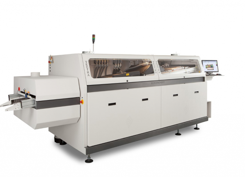
Mixed Technology Assembly
Integration of SMT and through-hole components on the same board, including selective soldering and hand soldering.
Micro Component Placement
Capable of placing ultra-small components (01005, 0201) with high-speed precision.
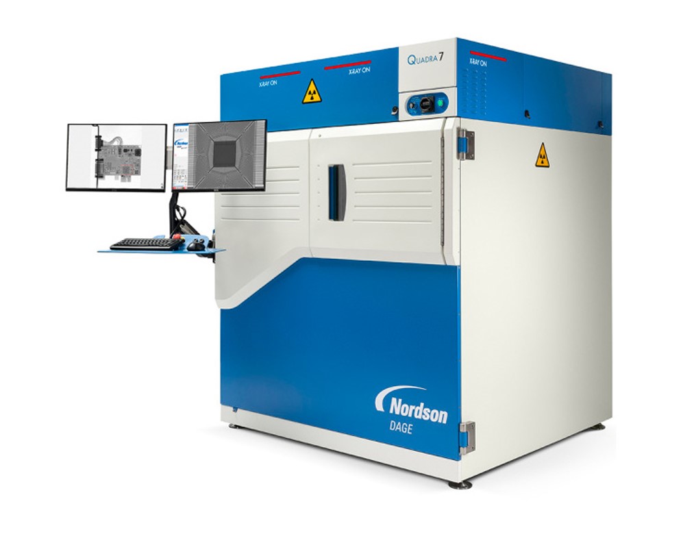
Complex Package Handling
Support for BGAs, QFNs, LGAs, CSPs, and PoP assemblies with X-ray verification.
Lead-Free and Leaded Processes
Separate lines for RoHS-compliant and traditional tin-lead soldering to prevent cross-contamination.
Flexible Volume Production
From quick-turn prototypes to high-volume production runs with scalable line configurations.
Inspection and Quality Control
+ 查看更多
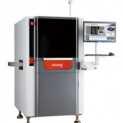
Solder Paste Inspection (SPI)
+ 查看更多
3D inspection of solder paste deposits for volume, height, and alignment before component placement.
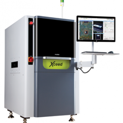
Automated Optical Inspection (AOI)
+ 查看更多
High-resolution cameras detect solder defects, polarity issues, and component misalignment.
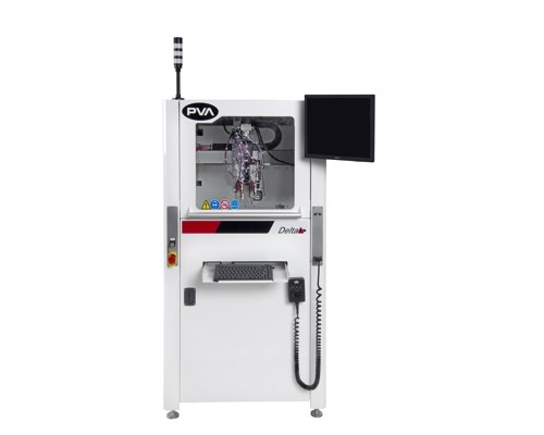
X-Ray Inspection
+ 查看更多
Non-destructive imaging for hidden joints (e.g., BGAs, LGAs) to detect voids, bridging, and cold solder joints.
In-Circuit Testing (ICT)
+ 查看更多
Electrical testing of individual components and nets using bed-of-nails or flying probe systems.
Functional Testing (FCT)
+ 查看更多
Simulates real-world operating conditions to verify board functionality, firmware, and I/O behavior.
Environmental Testing (optional)
+ 查看更多
Thermal cycling, vibration, humidity, and salt fog testing for ruggedized applications.
Feature | Specification |
Top Speed | Up to 77,000 CPH using 16‑nozzle head |
Placement Accuracy | ±25 µm (chips), ±40 µm general |
Component Size Support | From 03015 mm to 150 × 25 × 30 mm |
PCB Support | Up to 750 × 550 mm (single lane); dual‑lane up to 750 × 510 mm |
Inspection & Dispensing | Integrated SPI/AOI, non‑contact adhesive |
Feeder Capacity | Up to 120 tape feeders |
Special Features | Multi‑Recognition Camera, modular head/feeder system |
Feature | Specification |
Scan Speed | ~65 cm²/sec at 14 µm (~10 s per board 260×200 mm) |
Camera & Lighting | 4 MP CMOS, dual‑laser, RGBW + telecentric lens |
Height Accuracy / Repeatability | ±3 µm up to 3 mm; ~6 µm above |
Defect Types | Full range: solder, component alignment, OCR/OCV text, tombstone, bridging, warpage, foreign material |
Barcode Recognition | 1D/2D/QR + bad mark scanning |
Model Variants | Xceed (various sizes), Xceed II, Xceed II MP |
Advanced Sensor | TRSC‑II sensor in Xceed II: 4–14 µm selectable resolution |
Multi‑Process Support | SPI + AOI + CCI unified in Xceed II MP |
System Integration | SECS/GEM, TCP/IP, MES/ERP, web/mobile monitoring |
Feature | Specification |
Inspection Speed | Orange: 100 cm²/sec; Blue: 60 cm²/sec (10×10 µm) |
Transport Speed | Up to 1,000 mm/sec |
Height Accuracy / Repeatability | ~2 µm / <1 µm (3σ) |
Warpage Compensation | ±5 mm tracked in real time |
Defect & Measurement Types | Height, area, volume, offset, bridges, warpage, shrink, etc. |
PCB Compatibility | All board colors, finishes, reflective materials |
Software Analytics | SPC, process feedback, root-cause analysis |
Ease of Programming | Gerber/CAD/BOM import, auto-generated ROIs |
Model Variants | Sigma X, X Dual/Duo, XL, XXL, XXXL |
Max Panel Size | Up to ~1,200 × 450 mm depending on model |
Feature | Specification |
Feature resolution | Down to 0.35 µm at 10 W (0.95 µm at 20 W) |
Detector & Magnification | AspireFP™ 3 MP @25 fps; up to 45,000× |
Active stabilization | AXiS anti-vibration technology |
Inspection routines | BGA/QFN voids, wire sweep, pad, bump |
3D Options | X‑Plane® virtual slicing; µ‑CT available |
PCB sample size | Up to ~510 × 445 mm (tray); board size ~740 × 580 mm |
Platform software | Gensys control software, 24″ WUXGA display |
Feature | Specification / Capability |
Models Available | HPS5/55 (single-mode), HPS5/55 Dual-mode |
Dimensions | ~4,200 × 1,915 × 1,571 mm |
PCB Size Capacity | Up to ~510 × 510 mm |
Transport Width | Adjustable 50–510 mm |
Conveyor Height | 900 ± 20 mm |
Solder Pot Design | Electromagnetic pump |
N₂ Usage | ~1.5–2 m³/h per pot |
Module Options | 1, 2, or 3 solder modules |
Feature | Specification / Benefit |
Process Width | Up to ~508 mm (20") |
Preheat | Bottom up to 1.8 m; Top up to 1.2 m |
Solder Pot | Cast iron with lifetime warranty |
Solder Nozzles | UltraFill 4.0, DwellMax/Flex 4.0 |
Flux System | ServoJet / Spray / Sonic; dual-flux |
Flux Flow Monitoring | Non-contact, board-by-board monitoring |
Automatic Wave Height | ExactaWave with closed-loop control |
Wave Dynamics Control | Auto Exit Wing for flow adaptation |
Traceability | Data and SPC logging, barcode integration |
Nitrogen Option | Full or short tunnel for <50 ppm O₂ environments |
Benefit | Description |
Superior thermal uniformity | Ensures consistent solder profiles and minimizes defects |
Low maintenance & long life | Easy filter access and preventive flux capture |
Efficient energy use | Idle-saving features cut power use and reduce operational cost |
Lead‑free ready | Built to support lead‑free soldering, with tight process control |
Feature | Highlights |
Repeatability | ±25 µm with 5 µm resolution |
Motion Control | 3-axis gantry + optional 4-axis tilt/rotate |
Software | PathMaster® (offline programming, image import) |
Work Area | ~521 × 485 × 100 mm |
Throughput Speed | ~670 mm/s dispense, conveyor up to 24.4 m/min |
Applications | Conformal coating, potting, underfill, etc. |
Process Control and Traceability
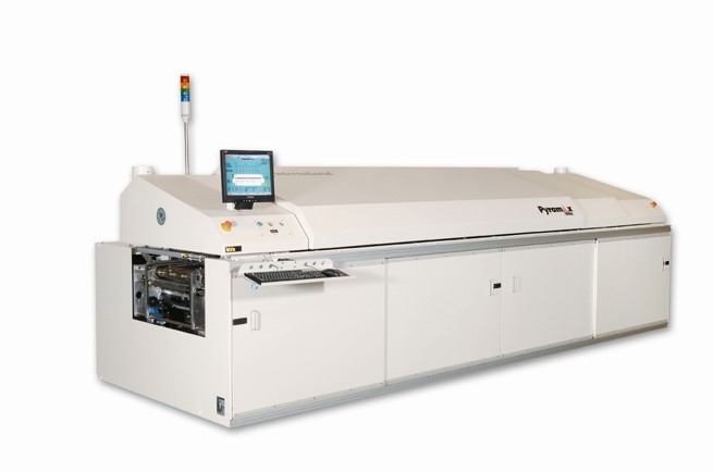
+ 查看更多
Reflow Profiling:
+ 查看更多
MES Integration:+ 查看更多
MES Integration:
+ 查看更多
ESD-Safe Environment: + 查看更多
ESD-Safe Environment:
+ 查看更多
Each board type receives a custom thermal profile to ensure optimal solder joint formation.
Our Manufacturing Execution System tracks every board through production, linking serial numbers to lot codes, operators, and inspection results.
Engineering Support
+ 查看更多
Design for Manufacturability (DFM)
+ 查看更多
Reviews to optimize PCB layout, component selection, and assembly processes.
Design for Testability (DFT)
+ 查看更多
Recommendations for test point placement and test strategy development.
Rapid Prototyping & NPI
+ 查看更多
Fast-turn builds with engineering feedback to accelerate product development cycles.
Stencil Design & Optimization
+ 查看更多
Custom stencil creation for precise solder paste application and consistent reflow results.
Component Engineering
+ 查看更多
Reviews to optimize PCB layout, component selection, and assembly processes.
Production Flexibility
+ 查看更多
Low to High Volume:
+ 查看更多
Quick Turnaround:
+ 查看更多
Whether you need 10 boards or 100,000, our flexible lines and scalable processes adapt to your production needs.
We offer expedited services for urgent builds without compromising quality.
Industries Served
+ 查看更多
Automotive & EV
+ 查看更多
Medical Devices
+ 查看更多
Industrial Automation
+ 查看更多
Telecommunications
+ 查看更多
Consumer Electronics
+ 查看更多
Aerospace & Defense
+ 查看更多


